3DNANOMAG
The 3DNANOMAG project at TU Wien is dedicated to the investigation of novel phenomena in three-dimensional nanomagnetism.
For this, the project exploits 3D printing of magnetic materials, creating new types of devices for applications in spintronics.
Lead Location: Institute of Applied Physics, TU Wien (Vienna, Austria).
Funding: European Research Council (ERC) – Consolidator
Duration: 2021 – 2027


PRINTBOT
The PRINTBOT project researches on 3D-nanoprinting of multi-material structures via FEBID/FIBID to enable functional microrobots at the sub-cellular scale.
Magnetic microrobots: Helical and ciliary swimmers fabricated and tuned for efficient propulsion in fluids.
On-board heating: Integration of nano-/plasmonic antennas for localized, controllable heating.
Targeted interaction: Active capture and on-demand release of size-selected nanoparticles.
Lead Location: Institute of Electron Microscopy and Nanoanalysis, TU Graz (Graz, Austria).
Funding: European Research Council (ERC) – Starting Grant
Duration: 2026 – 2030
FELMI-ZFE
NanoDigiTech
(Applications of direct-write nanoscale materials to digital technologies)
The specific problems that we want to tackle in NanoDigiTech are: a) excess of energy consumption by current semiconductor technologies used for computation and memory tasks. b) Excess of defects in devices, associated to the use of resists along the current optical and electron-beam lithography processes. c) Limited throughput in some of the existing nanopatterning processes for the fabrication of devices in emergent digital technologies. d) Lack of lateral resolution and excess of invasiveness in the characterization of novel magnetic nanotextures.
We will challenge these limitations by addressing three specific subtopics with the aid of direct-write nanolithography techniques based on focused electron and ion irradiation technologies. Thus, we expect to provide the following specific contributions:
- Fabrication of gate-tunable JJs that could constitute the backbone of superconducting circuits harnessing quantum computation and quantum sensors.
- Development of novel magnetic tips for magnetic force microscopy that could characterize with unprecedented lateral resolution and low invasiveness novel magnetic textures to be used in non-volatile racetrack-like memories.
- Fabrication of resist-free electrical gates to be used on 2D materials-based emergent technologies.
Lead Location: University of Zaragoza (Zaragoza, Spain).
Funding: Spanish Ministry of Science
Duration: 2024 – 2027
VMAG
The VMAG project at TU Wien has as objective the investigation of magnetic microscopy techniques with 3D vector sensitivity.
For this, the project exploits the 3D printing of magnetic sensors.
Lead Location: Institute of Applied Physics, TU Wien (Vienna, Austria).
Funding: Austrian Research Promotion Agency (FFG)
Partners: University for Continuing Education Krems (Krems, Austria), University of Vienna (Vienna, Austria), c-sense (Wiener Neustadt, Austria)
Duration: 2024 – 2027

Fabrigate
(Device for fabrication of metallic electrical contacts and of gate contacts based on organometallic thin films)
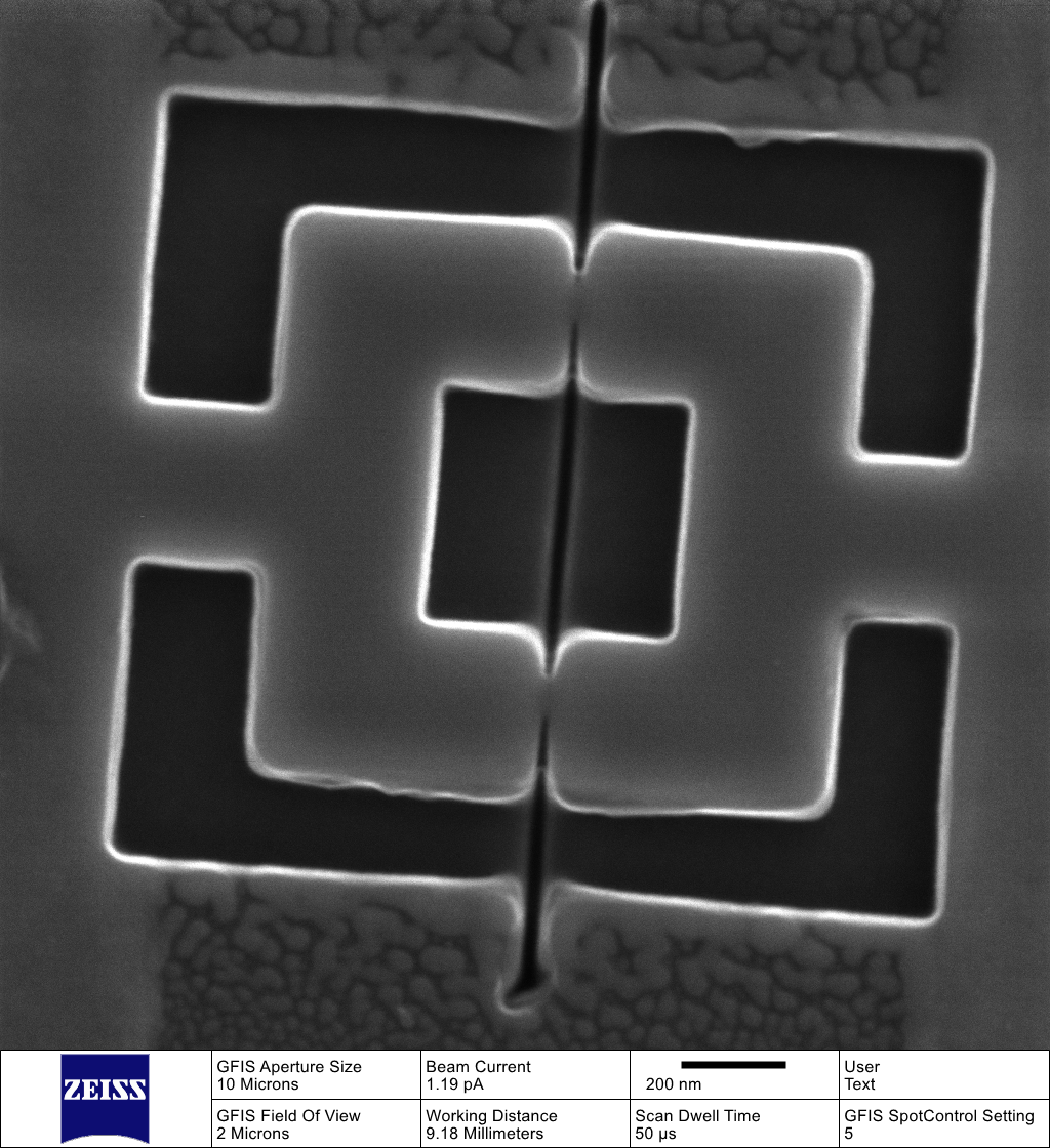
FABRIGATE aims to produce technological developments in two essential topics of the present and future semiconductor industry: the fabrication of metallic contacts and the fabrication of gate contacts. For that, we aim to apply the ideas collected in the patent Electrical contact manufacturing system and associated manufacturing method. The main problem identified in the current technology for growing metallic contacts/patterns is that the existing lithography processes are slow because several steps are required. This is the case for optical and electron-beam lithography, techniques in which we need to spin-coat a resist, perform the exposure to light or to electrons, carry out the resist development and finally do the etching step and the resist removal. In addition, it is well known that the use of resists leave residues on the surface which can be detrimental for the device functionality. The alternative strategy proposed in the FABRIGATE consists of the use of organometallic films, such as palladium acetate, which call for very low ion doses to create metallic structures. The facts that the organometallic film can be spin coated onto a full wafer, that the ion exposure dose is even smaller than that of PMMA-based electron-beam lithography and that the resolution is extremely good indicate that the proposed technology is potentially competitive for industrial application. In particular, our technology can be of interest for the following applications within these fields:
- Circuit edit: interconnects for integrated circuit reconfiguration, replacing beam-induced deposition processes in the gas phase.
- Mask repair: high-efficiency repair of (ultra-expensive) defective masks used in optical lithography for the fabrication of the integrated circuits.
- Metal contacts to semiconductor materials and 2D materials.
- Top and side gate contacts to field-effect-transistor architectures.
- Conductive transparent films for optoelectronics. -Quantum circuits for quantum technologies.
Lead Location: CSIC-University of Zaragoza (Zaragoza, Spain)
Funding: Spanish Ministry of Science
Duration: 2024 – 2025
MYRIAD
The MYRIAD project at TU Graz is driving advancements in micro- and nano-electronics, materials science, quantum technologies, and biotechnology through cutting-edge research and infrastructure development. By integrating novel structuring capabilities with state-of-the-art electron and ion beam microscopy techniques, MYRIAD enables the creation and analysis of complex 3D micro- and nanostructures with unprecedented material properties and functionality.
A core innovation of the project is its flexible use of various ion beams, such as Xe, Ar, N, and O, to achieve unparalleled precision in nanoscale fabrication. This capability supports transformative research in areas like energy solutions, quantum devices, and life sciences, bridging academic and industrial applications.
With its focus on fostering scientific collaboration and accelerating technology transfer, MYRIAD is not only advancing Austria’s research capabilities but also reshaping global perspectives on nanoscale innovation.
Lead Location: Graz Centre for Electron Microscopy (Graz, Austria)
Funding: European Regional Development Fund (ERDF), Austrian Research Promotion Agency (FFG)
Duration: 2024 – 2026

NanoTips
(Fabrication of ultra-sharp tips using electron and ion beams for AFM and their use in nanobiotechnology, nanomagnetism and SEM-AFM correlative microscopy)
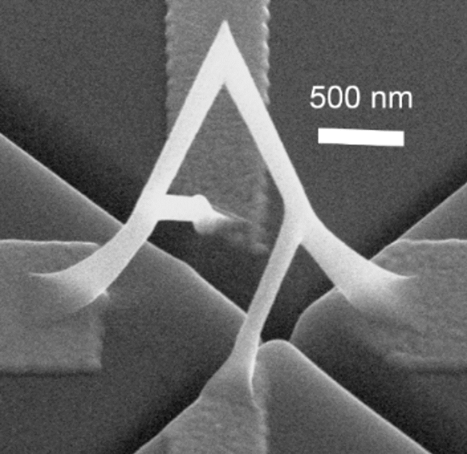
The NANOMIDAS research group is internationally recognized for the development of top-down nanofabrication processes, based on deposits induced by focused beams of electrons and ions (FEBID and FIBID). The FEBID and FIBID techniques allow the production of nanometric solid deposits (<10 nm) through the decomposition of a precursor gas with the electron/ion beam. These nanomaterials can present multiple functional properties: conductive, superconducting, plasmonic or magnetic. One of the most notable applications of the FEBID technique developed in recent years has been its use in the manufacture of ultra-sharp tips to provide high resolution and other advantages to AFM experiments. This method allows the local growth of a deposit using FEBID to functionalize the tip of a microlever of those used in the AFM technique. We will apply these nanotips to investigate:
- The dynamic behaviour of biomolecules in solution
- Structural effects in cells
- The magnetization state of ion-irradiated magnetic thin films
- The functional properties of surfaces through correlative AFM-SEM imaging.
Lead Location: CSIC-University of Zaragoza (Zaragoza, Spain)
Funding: Spanish Ministry of Science
Duration: 2024 – 2026
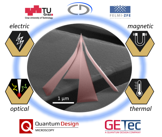
Christian Doppler Laboratory – DEFINE
The Christian Doppler Laboratory DEFINE focused on resaerch of innovative 3D nanoprobe concepts for advanced atomic force microscopy (AFM), fabricated via 3D nanoprinting using FEBID.
In collaboration with industry partners GETec Microscopy (now Quantum Design Microscopy) and Anton Paar, the lab created high-performance 3D nanoprobe concepts with unique electrical, magnetic, optical, and thermal functionalities. These advances enabled nanoscale measurements with unprecedented resolution and versatility. A particular highlight was the development of multifunctional probes combining several properties in a single tip, paving the way for simultaneous multimodal analysis.
The results gathered in the CDL DEFINE directly fed into the commercial FUSIONScope™ platform, marking a successful technology transfer from research to industry and establishing TU Graz as a hotspot in 3D nanoprinting.
Lead Location: Institute of Electron Microscopy at Graz University of Technology (Graz, Austria) in collaboration with the Graz Centre for Electron Microscopy (Graz, Austria)
Funding: Christian Doppler Association (CDG)
Duration: 2018 – 2025
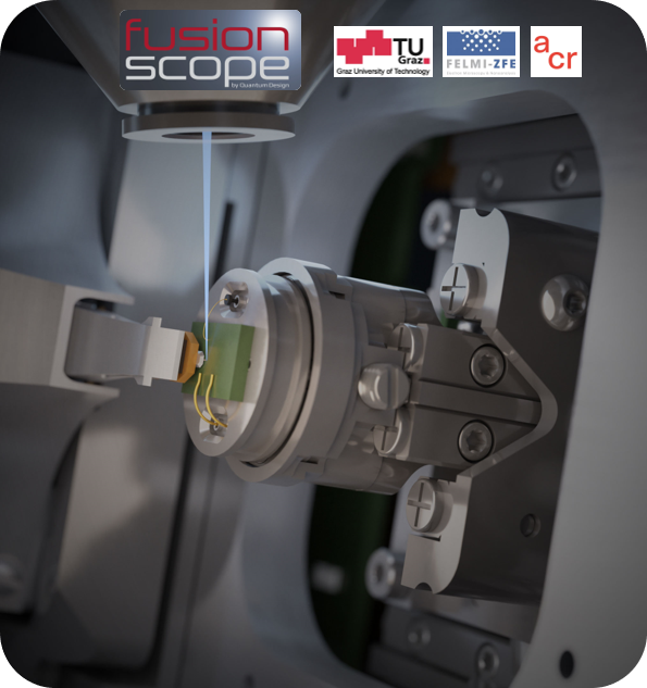
FUSION
The FUSION project at TU Graz is dedicated to revolutionizing the field of microscopy by seamlessly integrating advanced electron and ion beam technologies with cutting-edge analytical methods. This unique approach combines imaging, nanofabrication, and in situ analysis into a unified platform, enabling researchers to investigate materials with unprecedented precision and depth at the nanoscale.
FUSION focuses on enhancing correlative workflows, allowing the simultaneous exploration of structural, chemical, and functional properties of materials. By bridging disciplines, it opens new frontiers in materials science, nanotechnology, and life sciences, supporting breakthroughs in areas such as advanced materials development, nanoscale devices, and biomedical applications.
With its emphasis on innovation and interdisciplinary collaboration, the FUSION project is not just advancing the state-of-the-art in microscopy—it is reshaping how scientists interact with and understand the nanoscale world.
Lead Location: Graz Centre for Electron Microscopy (Graz, Austria) in collaboration with Institute of Electron Microscopy at Graz University of Technology (Graz, Austria)
Funding: Austrian Cooperative Research (ACR)
Duration: 2022 – 2024