
ELISA – Meeting
Join ELISA, a joint event bringing together LE2AP, LEELIS, and the former FEBIP meeting under the shared theme “Electrons in Lithography and Imaging for Science and Applications.”
ELISA 2026 spans the full landscape of electron-based science and technology, from the fundamental processes that govern electron–matter interaction to the instruments and applications that translate this understanding into imaging, patterning, and nanomanufacturing.
Rapid advances in beam technologies, resist materials & precursors, and data- / feedback-driven control are redefining how we understand and exploit electron-matter interactions. By merging the traditions of LE2AP, LEELIS and FEBIP, the meeting creates a unified space where modelling, metrology, experiments, and instrumentation converge – bridging physics and fabrication, materials and devices, and concepts and implementation. This perspective maintains the LE2AP+LEELIS initiative while including multi-material, hybrid 3D nanostructures central to the Beam Induced Nano-Manufacturing community.
The meeting fosters dialogue between foundation science and applications, strengthens bridges across core disciplines, and promotes shared terminology, metrology and benchmarking. It encourages collaboration among academia, industry, and instrument developers, offers visibility and networking.
Importantly it offers continuity as an excellent platform for early-career researchers and students for interaction with established academic research groups and industry, and helps shape a collective vision for next-generation electron-based science and technology.
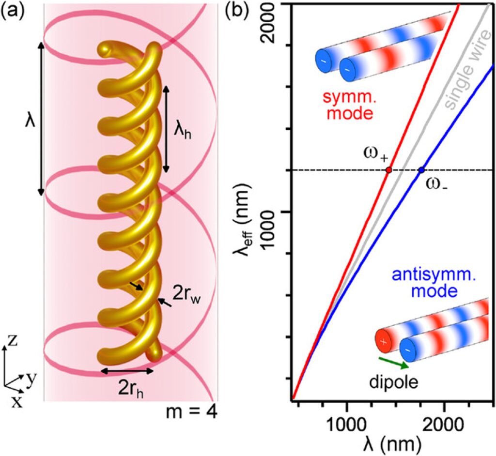
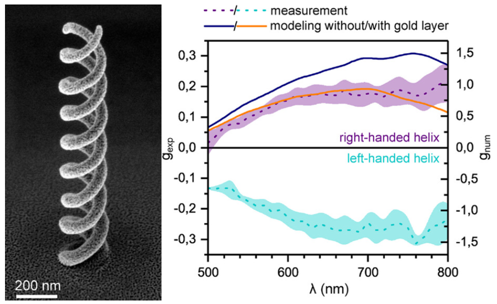
Double Helical Plasmonic Antennas
Aleksei Tsarapkin, Luka Zurak, Krzysztof Maćkosz, Lorenz Löffler, Victor Deinhart, Ivo Utke, Thorsten Feichtner, Katja Höflich

Adv. Funct. Mater. (2026), 2507471.
Plasmonic double helical antennas are a means to funnel circularly polarized light down to the nanoscale. Here, an existing design tool for single helices is extended to the case of double helices and used to design antennas that combine large chiroptical interaction strength with highly directional light emission. Full-field numerical modeling underpins the design and provides additional insight into surface charge distributions and resonance widths. The helical antennas are fabricated by direct writing with a focused electron beam, a technique that is unrivaled in terms of spatial resolution and 3D shape fidelity. After the printing process, the structures are purified using ozone plasma at room temperature, resulting in the smallest continuous double helix antennas ever realized in gold. Fabricated antennas are studied regarding their polarization-dependent transmission behavior, which shows a large and broadband dissymmetry factor in the visible range. Since the polarization of light is an important tool for implementing logic functionality in photonic and quantum photonic devices, these helices are potential building blocks for future nanophotonic circuits, but also for chiral metamaterials or phase plates.
Reconfigurable 3D Magnetic Nanoarchitectures
Fabrizio Porrati, Michael Huth
Journal of Applied Physics (2026), 139, 185103.
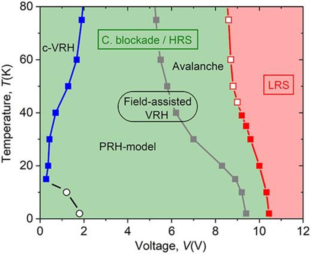
The charge-transport properties of nanogranular metals, comprising arrays of metallic nanoparticles embedded in an insulating matrix, are governed by the average tunneling conductance g between neighboring particles. In the weak-coupling limit (g ≪ 1), a transition from a high-resistive state (HRS) to a low-resistive state (LRS) occurs for bias voltages exceeding the global Coulomb-blockade threshold Vt. In this work, we investigate the charge-transport properties of Pt–C granular metals fabricated by focused electron beam induced deposition, across a bias voltage range spanning from the low-voltage regime (V ≪ Vt) up to the global Coulomb-blockade threshold (V ∼ Vt). Current–voltage characteristics (I–V), measured between room temperature and 2 K, reveal ohmic behavior at low bias voltages and field-assisted ohmic conduction at intermediate biases. Approaching Vt, the I–V curve exhibits a steep, non-linear increase in current, indicative of an avalanche-like charge carrier multiplication process. Above Vt, ohmic behavior is again observed. The resistive switching mechanism is hysteretic, exhibiting distinct transition voltages for the HRS-to-LRS and LRS-to-HRS transitions. Temperature-dependent conductivity measurements for V ≪ Vt reveal transport characterized by correlated variable-range hopping (c-VRH), indicative of cotunneling. At higher bias voltages, a field-assisted c-VRH regime is observed at low temperatures, which culminates in an abrupt transition to a low-resistance state at Vt. Finally, as the coupling strength between particles in Pt–C can be precisely controlled via electron curing, the switching temperature between HRS and LRS is adjustable from a few Kelvin to 60 K.
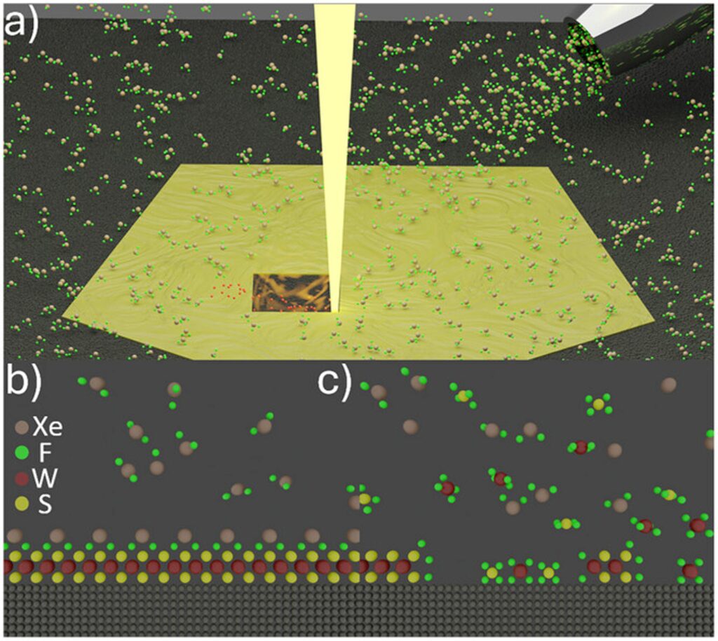
Nanoscale Editing of Multi and Single Layer Tungsten Disulfide via Gas-Assisted Focused Electron Beam Induced Etching for Device Prototyping
B. Spencer Gellerup, John C. Lasseter, Kyungnam Kang, Kai Xiao, Eva Zarkadoula, Jingsong J Huang, Scott T. Retterer, Steven J. Randolph, Philip D. Rack
Adv. Funct. Mater. (2026), e07816.
Focused electron beam induced etching (FEBIE) with XeF2 (xenon difluoride) precursor is conducted on multi-layer exfoliated WS2 (tungsten disulfide) and monolayer WS2 grown by chemical vapor deposition (CVD). The films are characterized by atomic force microscopy (AFM) and Raman and photoluminescence (PL) spectroscopy post-etching. The etch rates/efficiencies are reported as a function of electron beam energy, current, dwell time, and XeF2 pressure. Bulk film Raman spectra are unchanged post-FEBIE, indicating minimal subsurface damage. Monolayer WS2 shows a decrease in Raman and PL intensity post-FEBIE, with a dose-to-clear of ≈2 nC µm−2. The study reveals regimes affected by the various mass transport contributions such as refresh time and the ratio of electrons/XeF2. Spontaneous etching was discovered during FEBIE of large patterned areas due to the long frame/refresh times. Density functional theory and ab initio molecular dynamics simulations compares desorption of SFx and WFx molecules from pristine WS2 basal planes and pore edges, revealing the spontaneous etching is consistent with etching of partially etched monolayers during each frame. Single-line etching width of 21 nm, and patterning flakes into 100 nm wide channels are demonstrated. This work demonstrates the possibility of editing WS2 flakes into electronic devices of arbitrary dimensions for semiconductor applications.
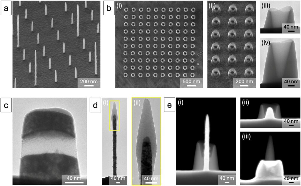
New Directions in Focused Ion Beam Induced Deposition for the Nanoprinting of Functional 3D Heterostructures
Frances Isabel Allen
Adv. Mat. Technologies (2026), e02542.
The focused ion beam (FIB) microscope is well established as a high-resolution machining instrument capable of site-selectively removing material down to the nanoscale. Beyond subtractive processing, however, the FIB can also add material via a technique known as focused ion beam induced deposition (FIBID). Using FIBID, the FIB can thus be employed for the direct-write of complex nanostructures. This work explores new directions in three-dimensional FIBID nanoprinting, harnessing unique features of helium and neon FIBs. In particular, the superior spatial resolution of these novel FIBs is leveraged to fabricate precise multimaterial architectures, an isotope effect is used to create satellite deposits, and dose-controlled implantation of the gaseous ions is used to engineer internal voids. In the context of voids, the fabrication of hollow nanopillars by helium-FIBID due to concurrent milling (as shown previously by others) is revisited. Insight into the chemical and structural composition of the nanostructures is obtained using advanced electron microscopy, accurately revealing buried interfaces, crystallite distributions, chemical compositions, and material transformations. Next-generation devices and technologies that could be enabled by the novel heterostructures demonstrated here are discussed, setting the stage for the potential evolution of FIBID into a versatile platform for functional nanomaterials design and fabrication.
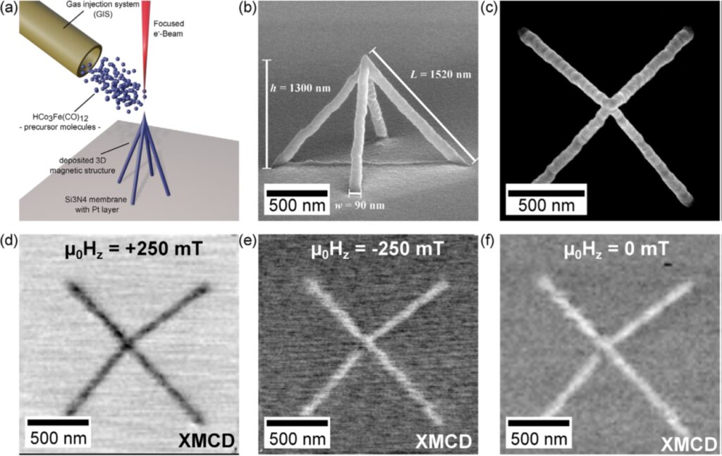
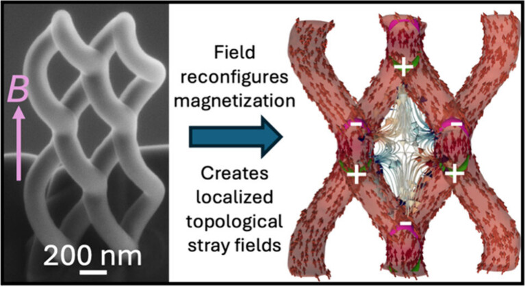
Reconfigurable 3D Magnetic Nanoarchitectures
Sabri Koraltan, Fabrizio Porrati, Robert Kraft, Sven Barth, Markus Weigand, Claas Abert, Dieter Suess, Michael Huth, Sebastian Wintz
Adv. Funct. Mater. (2025), 2501615.
3D nanomagnetism is a rapidly developing field within magnetic materials research, where exploiting the third dimension unlocks opportunities for innovative applications in areas such as sensing, data storage, and neuromorphic computing. Among various fabrication techniques, focused electron beam-induced deposition (FEBID) offers high flexibility in creating complex 3D nanostructures with sub-100 nm resolution. A key challenge in the development of 3D nanomagnets is the ability to locally control the magnetic configuration, which is essential to achieve desired functionalities. In this work, the magnetization reversal mechanism of a 3D nanoarchitecture fabricated using focused electron beam-induced deposition is investigated by combining direct observation via scanning transmission X-ray microscopy with finite element micromagnetic simulations. In particular, the investigation shows that the magnetization of the components of a 3D Co3Fe ttetrapod can be reversed individually and sequentially. Finally, it is demonstrated that complete control and reconfigurability of the system can be achieved by tuning the direction of the applied magnetic field.
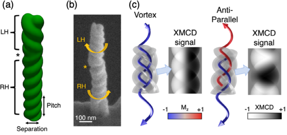
Fractional Skyrmion Tubes in Chiral-Interfaced 3D Magnetic Nanowires
John Fullerton, Naëmi Leo, Jakub Jurczyk, Claire Donnelly, Dédalo Sanz-Hernández, Luka Skoric, Nicholas Mille, Stefan Stanescu, Donald A MacLaren, Rachid Belkhou, Aurelio Hierro-Rodriguez, Amalio Fernández-Pacheco
Adv. Funct. Mater. (2025), 2501615.
Magnetic skyrmions are chiral spin textures with rich physics and great potential for unconventional computing. Typically, skyrmions form in bulk crystals with reduced symmetry or ultrathin film multilayers involving heavy metals. Here, the formation of fractional Bloch skyrmion tubes at room temperature is demonstrated by 3D printing ferromagnetic double-helix nanowires with two regions of opposite chirality. Using X-ray microscopy and micromagnetic simulations, it is shown that the coexistence of vortex and anti-parallel spin states induces the formation of fractional skyrmion tubes at zero magnetic fields, minimizing the energy cost of breaking the coupling between geometric and magnetic chirality. Control over zero-field states is also demonstrated, including pure vortex, or mixed skyrmion-vortex states, highlighting the magnetic reconfigurability of these 3D nanowires. This work shows how interfacing chiral geometries at the nanoscale can enable advanced forms of topological spintronics.
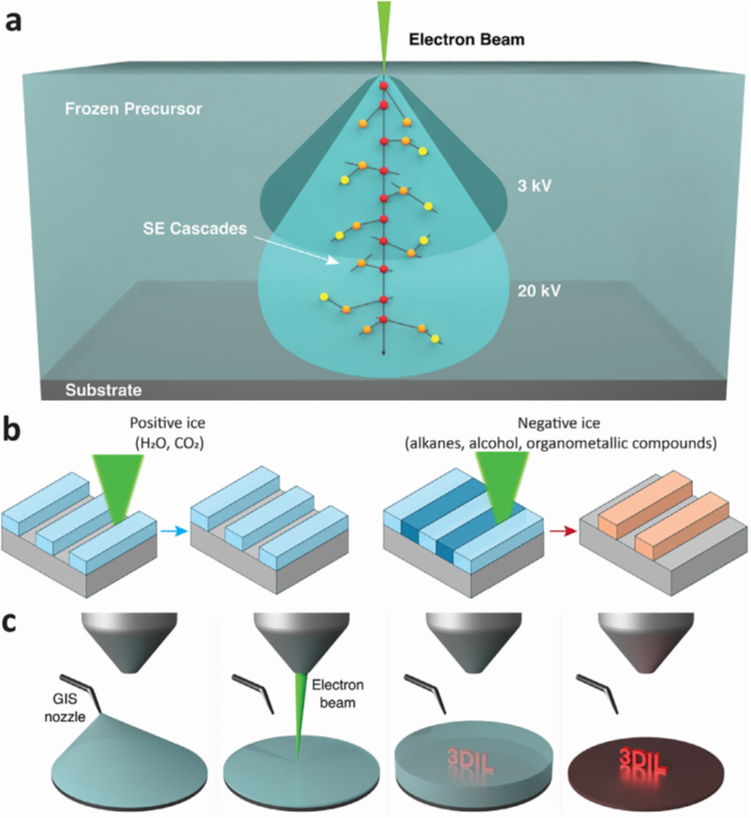
Ice Lithography: Recent Progress Opens a New Frontier of Opportunities
Bingdong Chang, Gwendoline A. E. Anand, Rubaiyet Haque, Dylan A. Chiaro, Mona Sharma, Andrew R. Williams, Frank Niklaus, Daryl W. Yee, Gavin M. King, Anpan Han
Adv. Funct. Mater. (2025), e15237.
Ice lithography (IL) is an emerging and versatile direct write method that complements two photon lithography and focused electron beam induced deposition (FEBID). Based on interaction between energetic electrons and frozen materials, IL permits the creation of high-resolution 2D patterns and intricate 3D micro- and nanostructures. This review highlights advancements spanning the past five years. Several notable breakthroughs have been reported during this time frame including the development of i) new classes of low-toxicity IL materials, including organometallics and renewable materials such as CO2 and ethanol; ii) innovative new substrates such as biological materials and even living micro-organisms; iii) disruptive processes, hardware and digital methods to obtain complex 3D objects; and iv) cutting-edge applications in 2D materials research, direct synthesis of quantum dots for sensing, and ultra-high density data storage. These discoveries offer the opportunity to focus on exciting future applications, and this review peeks into the future through a roadmap on how recent progress in IL might enable innovations into apparent unrelated fields of cancer screening, fundamental biophysics, quantum technology, future microsensor production, and more generally advanced functional materials research.
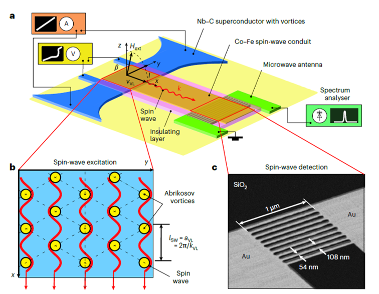
Moving Abrikosov Vortex Lattices Generate Sub-40-nm Magnons
Oleksandr V. Dobrovolskiy, Qi Wang, Denis Yu. Vodolazov, Roland Sachser, Michael Huth, Sebastian Knauer, Alexander I. Buzdin
Nat. Nanotechnol. (2025), doi.org/10.1038/s41565-025-02024-w.
Magnons, the quasi-particles of spin waves, are promising candidates for developing wave-based computing and hybrid quantum technologies. However, generating short-wavelength magnons through microwave excitation becomes increasingly challenging because the excitation efficiency decreases as the antenna size shrinks. Here we demonstrate an alternative approach and generate magnons in a Co–Fe strip using magnetic flux quanta, that is, Abrikosov vortices, moving in an adjacent Nb–C superconductor at velocities exceeding 1 km s−1. The moving vortex lattice acts on the magnetic layer via both static and dynamic stray fields. Our experiments showcase the unidirectional excitation of sub-40-nm wavelength magnons and their coherent interaction with the moving vortices. In turn, the Nb–C sustains its low-resistive state because the magnon creation removes energy from the superconductor. This discovery enables high-speed on-chip electrically driven magnon generation and validates an alternative means of magnon excitation. Our approach could be adapted to other wave excitations, such as surface acoustic waves, for integration into advanced electronic and hybrid quantum systems.

Beyond the Beam: Exploring Charged Particle Nanoprinting
Nicolas Paul Jochmann, Alba Salvador-Porroche, Sven Barth
Adv. Funct. Mater. (2025), e07465.
Charged particle nanoprinting using electrons and ions has advanced significantly, presenting vast opportunities for both scientific research and industrial applications. This perspective outlines the fundamental principles of these processes to provide context for recent advancements and suggests strategies to ensure that these well-established techniques continue progressing in the rapidly evolving field of nanoprinting. Despite substantial progress, fundamental challenges remain, requiring further optimization. In Focused Electron Beam Induced Deposition (FEBID) and Focused Ion Beam Induced Deposition (FIBID), the tailoring of precursor molecules is crucial for achieving high-purity materials or composites with specific functional properties. Optimizing ligand stability, fragmentation efficiency, and bond strength in precursors necessitates refined precursor design and careful selection of deposition parameters. For instance, the use of reactive ions in plasma FIB/SEM systems, for example, offers promising opportunities for expanding FIBID’s role in material engineering. Furthermore, the microstructures of both as-grown and processed nanodeposits are analyzed and discussed considering fundamental driving forces. Additionally, hybrid techniques utilizing nanoprinted materials for the fabrication of heterostructures with tailored and diverse functional properties are explored. This rapidly advancing field of nanoprinting thrives on interdisciplinary collaboration, fostering innovation, and pushing the limits of nanoscale manufacturing.
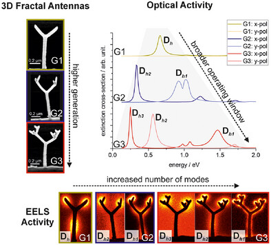
The Realization of Multidirectional, Free-Standing 3D Plasmonic Nanostructures via 3D Nanoprinting: A Case Study of Fractal Antennas
Verena Reisecker, Robert Winkler, Ulrich Hohenester, Evelin Fisslthaler, Daniel Knez, Gerald Kothleitner, Georg Haberfehlner
Adv. Funct. Mater. (2025), e15339.
This study demonstrates the realization of precisely engineered 3D plasmonic nanostructures capable of manipulating and redirecting optical signals in 3D space. Lifting nanostructures into the third dimension can significantly extend current excitation/emission possibilities and signal strength, due to increased design freedom and reduced substrate influence. So far, the fabrication of metal-based 3D nanostructures poses significant challenges, attributed to either material or design. Herein, gold-based 3D nanostructures are deposited via Focused Electron Beam Induced Deposition (FEBID) and purified through etching in water vapor – a process particularly hard to control in the case of free-standing designs. By alternately irradiating the structures from opposing 90° side views, the impact of beam direction can be successfully leveraged, thereby ensuring efficient carbon removal without compromising structural fidelity. This newly introduced protocol is demonstrated for the case of fractal canopy trees, composed of free-standing nanowires with distinct lengths and diameters, oriented at defined angles to form fractal antennas of varying complexity. Plasmonic responses are evidenced both numerically and experimentally via excitation with fast electrons, showcasing broadband plasmonic activity, customizable polarizability and excellent agreement with simulation. This directional purification strategy now enables the reproducible fabrication of 3D plasmonic nanoarchitectures and is expected to significantly advance experimental capabilities and understanding in 3D nanoplasmonics.

Reconfigurable Three-Dimensional Superconducting Nanoarchitectures
Elina Zhakina, Luke Alexander Turnbull, Weijie Xu, Markus König, Paul Simon, Wilder Carrillo-Cabrera, Amalio Fernández-Pacheco, Uri Vool, Dieter Suess, Claas Abert, Vladimir M. Fomin, Claire Donnelly
Adv. Funct. Mater. (2025), 2506057.
When materials are patterned in 3D, there exist opportunities to tailor and create functionalities associated with an increase in complexity, the breaking of symmetries, and the introduction of curvature and non-trivial topologies. For superconducting nanostructures, the extension to the third dimension triggers the emergence of new physical phenomena, and lead to advances in technologies. Here, 3D nanopatterning is harnessed to fabricate and control the emergent properties of a 3D superconducting nanostructure. Not only are the existence and motion of superconducting vortices demonstrated in 3D but, with numerical simulations, it is shown that the confinement leads to well-defined bending of the vortices within the volume of the structure. This 3D confinement manifests experimentally in a strong geometrical anisotropy of the critical field, through which the reconfigurable coexistence of superconducting and normal states in the 3D superconducting architecture, and the local definition of weak links, are achieved. In this way, an intermediate regime of nanosuperconductivity is uncovered, where the vortex state is truly 3D and can be designed and manipulated by geometrical confinement. This insight into the influence of 3D geometries on superconducting properties offers a route to local reconfigurable control for future computing devices, sensors, and quantum technologies.
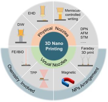
Nanoscale 3D Printing for Empowering Future Nanodevices
Yuxiang Yin, Bingyan Liu, Yaochen Han, Qiling Liu, Jiehao Kou, Yueqi Zhang, Ji Wen, Shihao Liu, Qingyan Wang, Yaotao Shan, Yizhou Liu, Jicheng Feng
Adv. Mater. Technol. (2025), 10, 2500083.
3D nanoprinting presents a fundamentally different approach (bottom-up) compared to traditional nanolithography (top-down), enabling the fabrication of nanostructures with greater material versatility and complex spatial geometries. Initially developed for macroscopic devices fabrication, 3D printing is now progressing toward the nanodevices production with active functionalities. This review explores cutting-edge 3D printing technologies for nanoscale materials, emphasizing key achievements, foundamental principles, and persisting technological challenges. This review discusses potential opportunities in material selection, electronic co-design, device integration, scalability, and essential steps toward commercialization. Among the numerous insightful reviews on 3D printing, this review aims to provide a more detailed discussion of the perspective and existing gaps in practical implementation, grounded in current technological capabilities. Furthermore, the future impact of 3D nanoprinting on academia and industry is explored.
Double Helical Plasmonic Antennas
A. Tsarapkin, L. Zurak, K. Maćkosz, L. Löffler, V. Deinhart, I. Utke, T. Feichtner, and K.Höflich
Adv. Funct. Mater. (2025), 2507471.
Plasmonic double helical antennas are a means to funnel circularly polarized light down to the nanoscale. Here, an existing design tool for single helices is extended to the case of double helices and used to design antennas that combine large chiroptical interaction strength with highly directional light emission. Full-field numerical modeling underpins the design and provides additional insight into surface charge distributions and resonance widths. The helical antennas are fabricated by direct writing with a focused electron beam, a technique that is unrivaled in terms of spatial resolution and 3D shape fidelity. After the printing process, the structures are purified using ozone plasma at room temperature, resulting in the smallest continuous double helix antennas ever realized in gold. Fabricated antennas are studied regarding their polarization-dependent transmission behavior, which shows a large and broadband dissymmetry factor in the visible range. Since the polarization of light is an important tool for implementing logic functionality in photonic and quantum photonic devices, these helices are potential building blocks for future nanophotonic circuits, but also for chiral metamaterials or phase plates.
Design and Control of Three-Dimensional Topological Magnetic Fields Using Interwoven Helical Nanostructures
J. Fullerton and C. Phatak
Nano Letters (2025), 25, 5148.
Three-dimensional (3D) magnetic nanostructures are an emerging platform capable of creating complex topological magnetic fields. The control of localized nanoscale magnetic fields is seen to be of importance for diverse areas from bioapplications such as drug delivery, to particle trapping and controlling Majorana Fermions for quantum computing. Three-dimensional geometric confinement and proximity can create tailor-made spin textures not possible in two dimensions. The control of magnetization afforded here can allow the formation of unique stray field textures. Here, we report the creation of reconfigurable 3D topological magnetic field textures induced by an interwoven 3D nanostructure and applied field protocol. These field textures emerge due to distinct DWs formed in this structure and lead to the creation of an antivortex field, a hexapole cusp and a 3D skyrmion field tube of mixed chirality. Our results therefore show a key step toward the design and control of topological magnetic fields on the nanoscale.
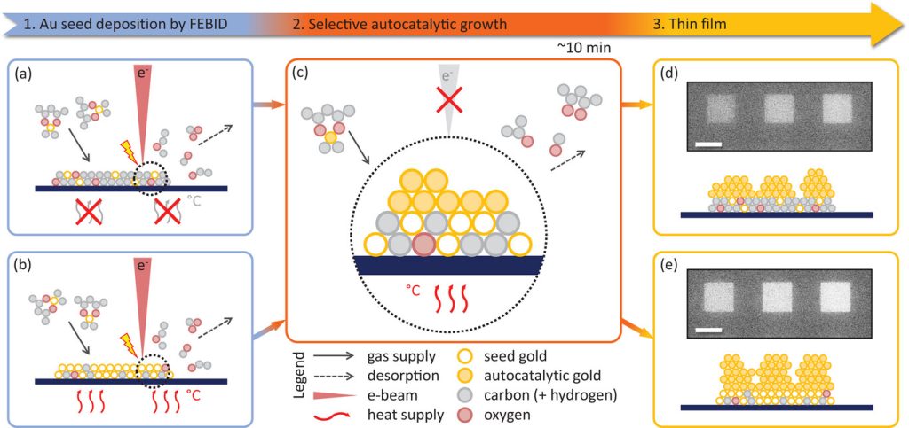
Area-Selective Chemical Vapor Deposition of Gold byElectron Beam Seeding
A. Tsarapkin, K. Maćkosz, C.S. Jureddy, I. Utke, and K. Höflich
Advanced Materials (2024), 36, 2313571.
Chemical vapor deposition (CVD) is an established method for producing high-purity thin films, but it typically necessitates the pre- and post-processing using a mask to produce structures. This study presents a novel maskless patterning technique that enables area-selective CVD of gold. A focused electron beam is used to decompose the metal–organic precursor Au(acac)Me2 locally, thereby creating an autocatalytically active seed layer for subsequent CVD with the same precursor. The procedure can be included in the same CVD process without the need for clean room lithographic processing. Moreover, it operates at low temperatures of 80 °C, over 200 K lower than standard CVD temperatures for this precursor, reducing thermal load on the specimen. Given that electron beam seeding operates on any even moderately conductive surface, the process does not constrain device design. This is demonstrated by the example of vertical nanostructures with high aspect ratios of ≈40:1 and more. Written using a focused electron beam and the same precursor, these nanopillars exhibit catalytically active nuclei on their surface. Furthermore, by using the onset of the autocatalytic CVD growth, for the first time the local temperature increase caused by the writing of nanostructures with an electron beam can be precisely determined.
A Review on Direct-Write Nanoprinting of Functional 3D Structures with Focused Electron Beams
V. Reisecker, R. Winkler, and H. Plank
Advanced Functional Materials (2024), 34, 2407567.
Following Moore`s law, the performance of devices should double within a two-year span, which can either be done by reducing the size of the individual components or adapting the working mechanism. In most cases the same mantra applies – pushing the size while keeping the quality. As manufacturing techniques are approaching the atomic scale, however, miniaturization reaches its intrinsic limit, shifting focus toward higher-dimensional architectures realized by stacking planar layers or fabricating true, free-standing nanostructures. A mask-less, additive manufacturing technique with the capability to produce such 3D structures at the nanoscale is called Focused Electron Beam Induced Deposition (FEBID). Applying a focused electron beam in a conventional scanning electron microscope together with a gaseous metal-precursor gives access to a vast library of complex, 3D nanostructures, which exhibit feature sizes down to the 10 nm-range and can be printed in a single step on most substrates. This review aims at introducing the technique to a broader scientific community, breaking down the most important processing routes and highlighting disciplines explored so far ranging from nanooptics and nanomagnetism, over scanning probes and field emitters to sensing and particle trapping. Finally, a future roadmap of the technique is discussed, and prospective research focus identified.